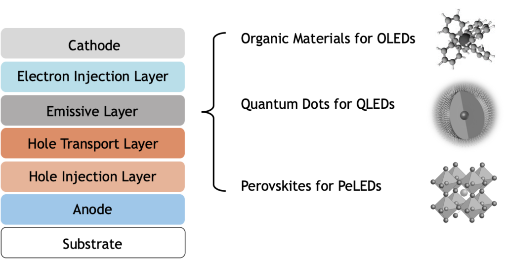
PeroLED Platform
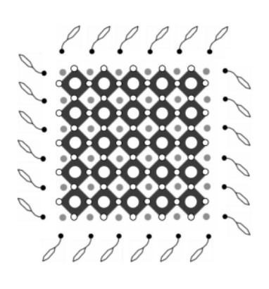
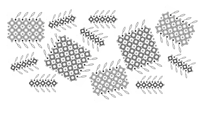
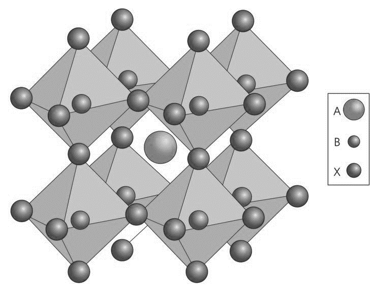
One extremely promising technique to expand the colour gamut of displays is to use perovskite light emitting materials. Perovskite materials are defined by their unique crystal structure of ABX3 where A and B are cations of different sizes, and X is an anion that bonds to A and B.
Excyton has developed a strong patent portfolio relating to the adoption of Perovskite LEDs (PeLEDs) in electronic displays. The patent portfolio covers perovskite ink formulations, device architectures, manufacturing methods and display designs.
Excyton has a particular focus on fabricating PeLEDs by inkjet printing and vacuum drying.
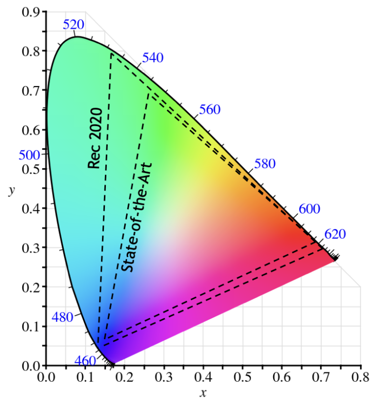
State-of-the-art displays, such as those in smartphones, tablets, watches, laptops, monitors and televisions are limited by their colourfulness. They can only render up to approximately 52% of colours visible to the human eye (as defined by the CIE 1931 (x, y) chromaticity diagram). The remaining colours are absent. This hinders the ability of displays to appear true to life and limits user experience. This is depicted in the chromaticity diagram, where only those colours contained in the “State of the Art” triangle can be rendered by state-of-the-art displays of today. This is the DCI-P3 colour gamut.
To address this shortfall, new standards have been introduced by ITU-R Recommendation BT.2020 (commonly known as BT. 2020 or Rec. 2020). These standards require displays of the future to render at least 76% of colours visible to the human eye. This is the Rec. 2020 colour gamut. This is depicted in the chromaticity diagram, where all colours contained in the “Rec 2020” triangle must be rendered for a display to meet Rec. 2020 standards. Perovskite LED technology provides a unique solution to enable displays to meet Rec. 2020 standards.
Perovskite Light Emitting Materials
Photoluminescent
Electroluminescent
Electroluminescent perovskite materials may be adopted in Perovskite Light Emitting Devices (PeLEDs). The red, green or blue pixels of a display may be individually patterned PeLEDs that emit light directly without the need for colour filters or colour conversion layers. This architecture is potentially more efficient than using Enhancement Films of Colour Conversion Layers. Excyton has developed technology and a patent portfolio with particular focus on electroluminescent perovskite materials and PeLEDs.